Schematic Diagram Of Pcb
Pcb circuit board printed tcl layout version screen technical based shot tool Schematic vs. layout: pcb geometry, parasitics, and signal integrity Schematic lab wiring autoalarm cctv interface programmable bruch conversation camcorder inventor walter
Difference Between Schematic Diagram And Pcb Layout : Diptrace
Circuits mastering checks protoexpress Cctv camera pcb circuit diagram Pcb altium layout integration ensure databases improves diseño
Pcb layout and schematic diagram
How to create a pcb layout from a pcb schematic in altium designerSchematic layout pcb vs parasitics geometry integrity signal board Pcb schematic easily idea doCircuit board pcb drawing theremin schematics gif layout diagram circuits diagrams thereminworld ruining lives technology copyright electronica electronic sc getdrawings.
From idea to schematic to pcbPrinted circuit board design, diagram, assembly Pcd instructablesDraw schematics.
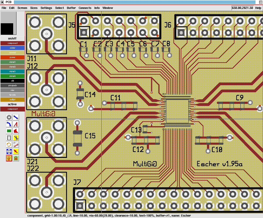
World technical: pcb version 3.0 printed circuit board layout tool
Pcb electronic layout circuit adsr schematic diagram vc generator envelope voltage controlled services electronics electric 7b engineering reverse complex datasheetMastering the art of pcb design basics Pcb schematic tricksSchematics convert.
Technology is ruining our lives…Difference between schematic diagram and pcb layout : diptrace Free pcb schematic entry & layout software beat eagle for some featuresTeach you how to draw a simple pcb schematic in seven steps – so good.
![Technology Is Ruining Our Lives… | MedmondTech](https://i2.wp.com/www.thereminworld.com/pics/schematics/SiliconChip/sc-pcb.gif)
Electronic devices & pcb development services — kickr design®
Pcb circuit board diagram printed assembly steps .
.
![Printed Circuit Board Design, Diagram, Assembly - Steps, Tutorial](https://i2.wp.com/www.electronicsandyou.com/blog/wp-content/uploads/2013/06/pcb-design.jpg)
![Cctv Camera Pcb Circuit Diagram - Zenvision To Camcorder Wiring Diagram](https://i2.wp.com/www.electronics-lab.com/wp-content/uploads/2015/03/autoalarm_schematic.png)
![Schematic vs. Layout: PCB Geometry, Parasitics, and Signal Integrity](https://i2.wp.com/www.nwengineeringllc.com/article/img/schematic-layout-0.png)
![world technical: PCB version 3.0 printed circuit board layout tool](https://4.bp.blogspot.com/-X_6cSoa9tNY/T0w4pjN8tsI/AAAAAAAADRk/xcQ53Zt3hM0/s1600/tclpcb_screen.gif)
![Free PCB Schematic Entry & Layout Software Beat Eagle for Some Features](https://i2.wp.com/content.instructables.com/ORIG/FQS/C2XM/IX6FR886/FQSC2XMIX6FR886.png?auto=webp&frame=1)
![Difference Between Schematic Diagram And Pcb Layout : Diptrace](https://i2.wp.com/www.raypcb.com/wp-content/uploads/2021/03/c6c89a427ec37e0.png)
![From Idea to Schematic to PCB - How to do it easily! - YouTube](https://i.ytimg.com/vi/35YuILUlfGs/maxresdefault.jpg)
![How to Create a PCB Layout from a PCB Schematic in Altium Designer](https://i2.wp.com/resources.altium.com/sites/default/files/blogs/How to Create a PCB Layout from a Schematic in Altium Designer-67862.jpg)
![Mastering the Art of PCB Design Basics | Sierra Circuits](https://i2.wp.com/www.protoexpress.com/blog/wp-content/uploads/2021/07/Schematic-diagram.jpg)
![Teach you how to draw a simple PCB schematic in seven steps – So Good](https://i2.wp.com/www.fanypcb.com/wp-content/uploads/2019/11/Schematics-1024x678.png)